In part one, I talked about the general process and some of the tools needed. Now it’s time to get down to business.
After you have a design done, the first thing to do is make a transparency. I found a few boxes of 3M film lying around. Now I hoard it.
I’m sure this can be purchased on Ebay or Amazon. It’s funny, I actually remember doing presentations on this stuff early in my career. I’ve tried a few other things like tracing paper, but nothing works like these. I won’t do it any other way.
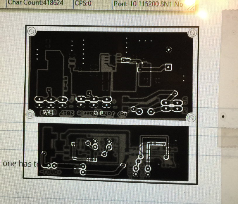
First order of business is to print/plot your artwork. I print a top and bottom separately. For the top, I select only the top layer, pads, and vias. Sometimes I also select some other layers like document if I want to etch on some artwork or text. Here are the minimum eagle layer settings for the top:
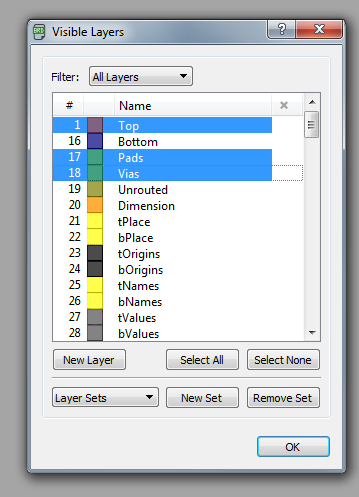
I use the same settings for the bottom, but turn off layer 1 and turn on layer 16.
For the actual printing, you want to select the “Black” and “Solid” checkbox options. I also select the “Mirrored” option for the Top layer. By doing that, you technically orient the printed side of the transparency closest to the board. I don’t know if it really makes a difference. It would be important if you were trying to do a toner transfer onto a bare copper board, but that’s not what we’re talking here….Make sure the scale factor is 1.
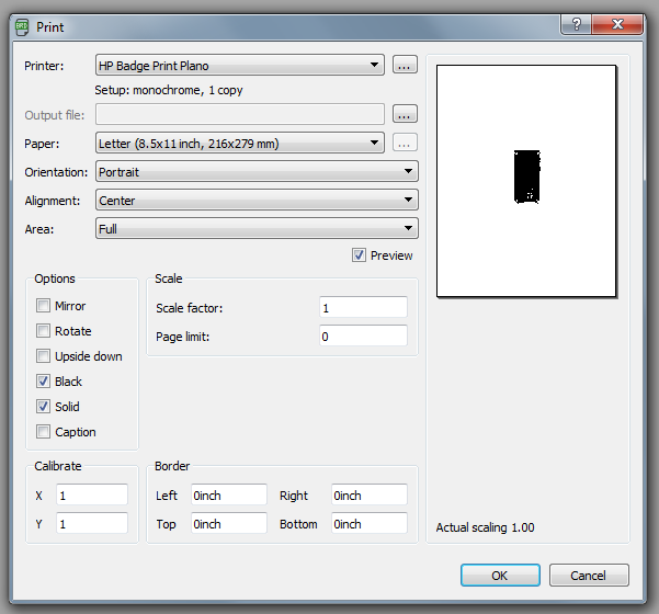
In terms of a printer, I’ve never gotten satisfactory results from an InkJet printer. The only thing I’ve gotten to work is a Laserjet, and I set it’s resolution at the highest setting I can find. I also tried printing it to a PDF and then printing elsewhere without an success. There are small errors that crop up and make the prints unusable. I suppose you could do Gerber files etc but I haven’t experimented with that yet.
Once you get the top and bottom transparencies printed, they need to be “sandwiched” together. In other words, the top layer transparency needs to be lined up with the bottom layer transparency to make a stack. The bare copper board will then be inserted between to make the “sandwich”.
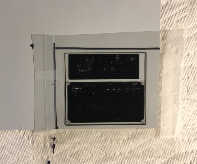
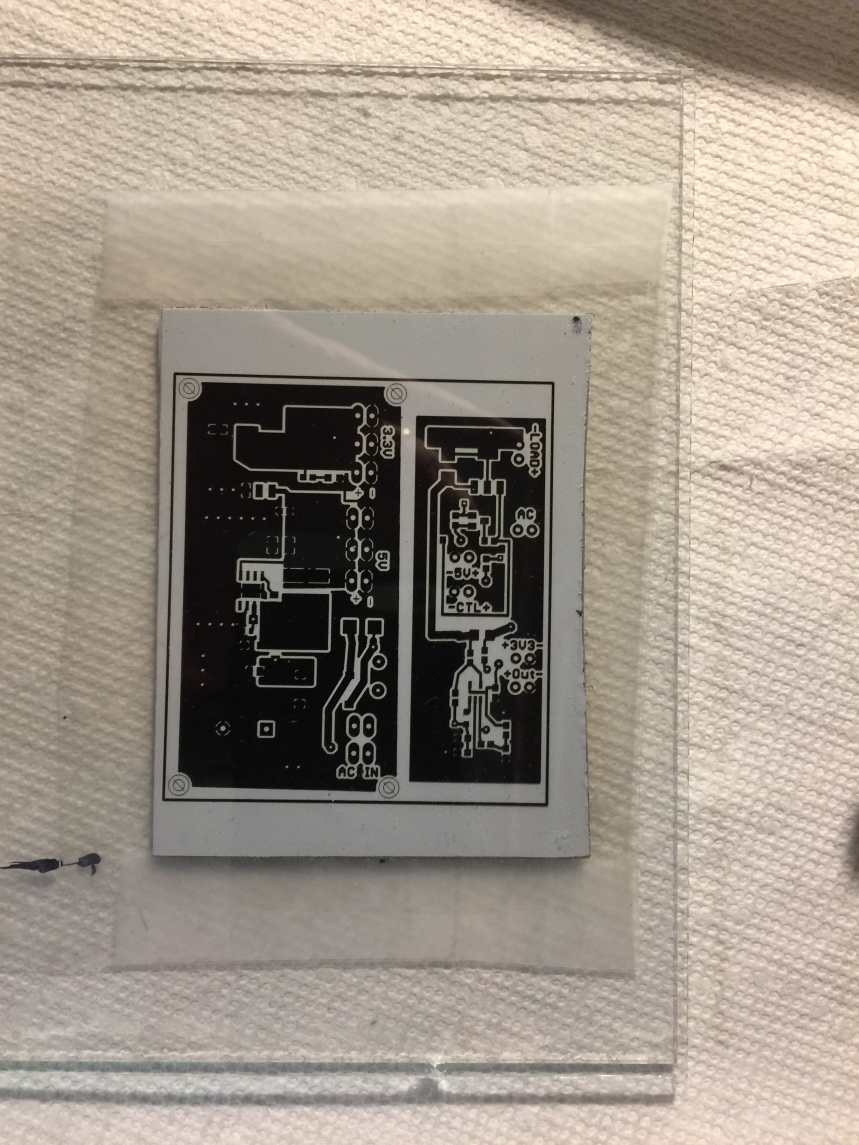
To do this, I take the top and bottom transparencies and cut them out, leaving a ~1.5” border on the bottom layer transparency and a larger (~2+”) border on the top layer. Here’s an example:
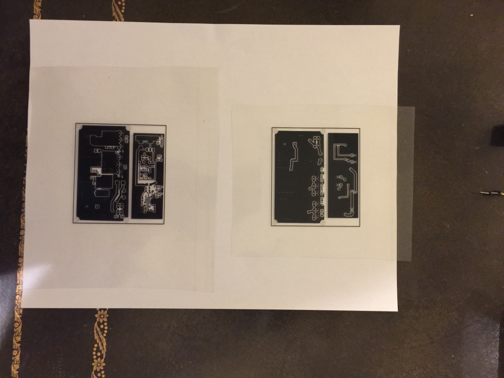
Top of board (Left) and bottom of board (Right). Note border on top and smaller border on right.
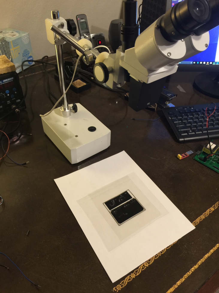
Next I align the top and bottom together. This is a very critical step and how you get your top and bottom holes to be lined up. I use a microscope to do this, but a very good light source can also work. Here’s a couple pics’s.
Bottom transparency over top transparency and aligned.
Once I get them aligned, I tape them along each side, but leave the top and bottom open.
Holding up the aligned and taped top and bottom transparency in front of a computer screen to get a good look at the finial alignment.
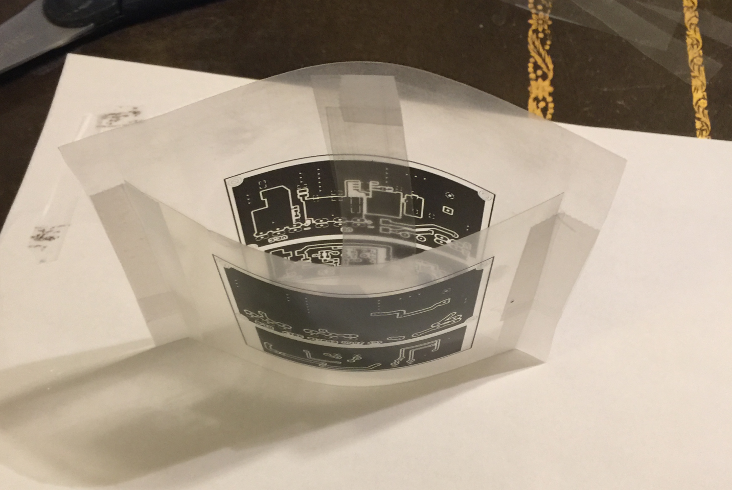
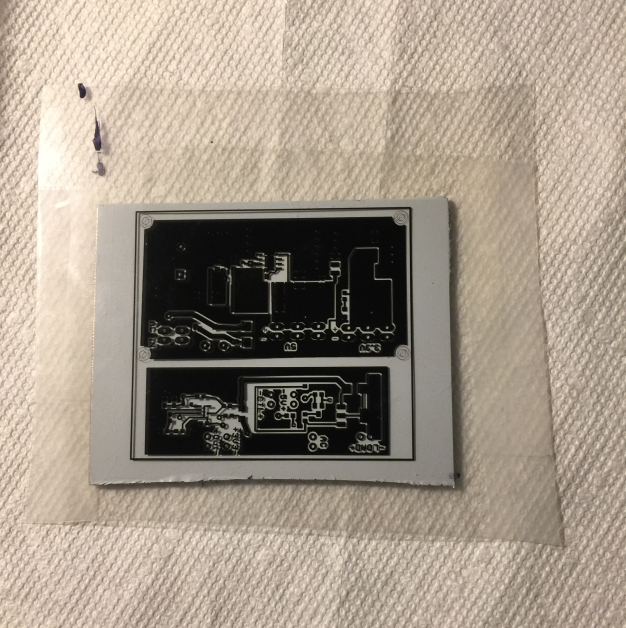
This makes it easy to see the finished and aligned artwork.
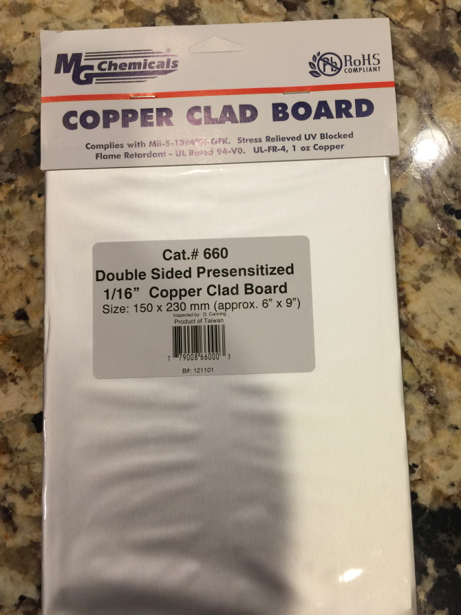
Next it’s time to cut the board out to be etched. I use pre-sensitized double sided board like this:
I simply take the artwork and hold it over the board, then mark the board with a permanent marker where it should be cut. I want the board to be larger than the artwork, but small enough to fit into the “sandwich”
Next, I use a cutting wheel to cut along the marks. Note: this makes more dust than you’d expect. The dust is mostly from the fiberglass PCB and probably not the greatest thing to breathe so take precautions.
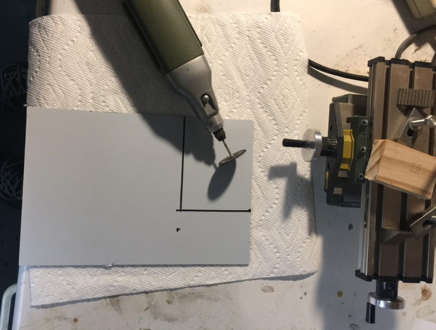
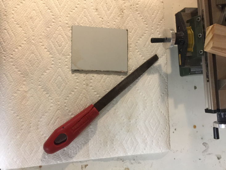
After cutting, I use a file to smooth the rough edges. This allows the board to fit better into the artwork “sandwich”, and makes for an easier piece to handle.
Here you can see the pre-sensitized board (with white protective film still attached) in the artwork sandwich. Also note, you see stuff sitting on paper towels a lot. I use them to keep stuff as clean as possible.
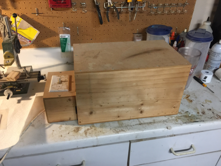
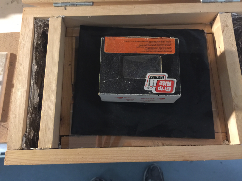
The next step is to expose the artwork “sandwich” to UV light. Here is a shot of the lightbox I built.
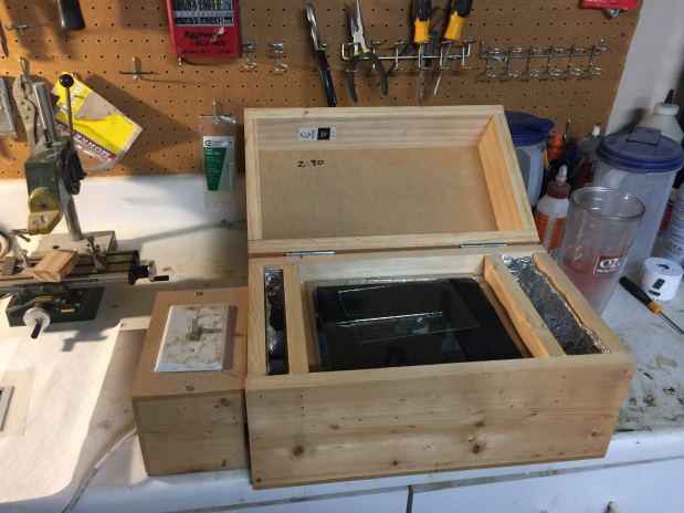
When it’s opened, the construction details are pretty easy to see. Note that on the inside of the lid the number 2:30 is written in marker. This is so I know to expose each PCB side exactly 2:30 each time. I arrived at that number through trial and error, basically trying different exposure times until I got the best artwork transfer. I suspect it’s a function of UV power, distance, pre-sensitized board coating etc. I’ve been using it a couple years now and it hasn’t changed. Yes, I thought of putting a cool microprocessor controller (or other electronics) on the light box to allow me to time the exposure and automatically do warm up and shut down. It’s just too easy to do it manually.
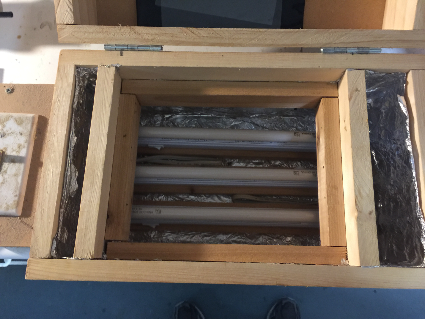
Looking inside the box, you can really see what’s going on. There is a frame which holds a piece of acrylic I got at Home Depot. https://www.homedepot.com/p/Plaskolite-8-in-x-10-in-x-0-050-in-Polystyrene-Sheet-1S08104A/202043333
Under the frame are 3 8W UVA bulbs I got here:
https://www.1000bulbs.com/product/3476/F-08T5BL.html
I bought 3 mini florescent fixtures at Home Depot and wired them in parallel and to a switch. Just for extra overkill, I lined the box with foil.
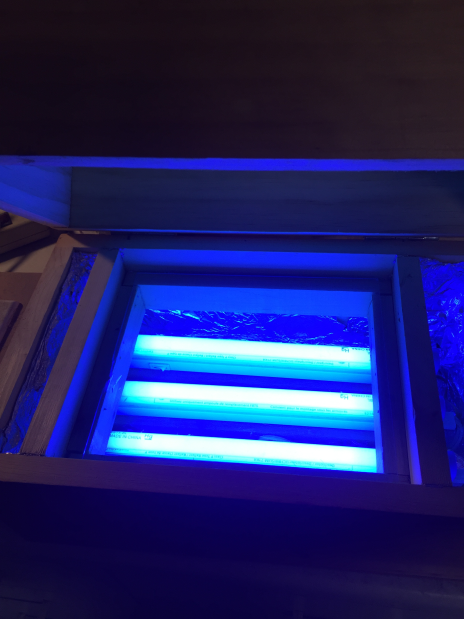
Here are the lights on…..which strangely gives me an urge to listen to some Zeppelin.
A final note on the light box, I’ve thought many times about adding another set of lights on the top so that I could do the top and bottom exposure at once. It would make the box bigger and more expensive to make, but would save a little time. Your call.
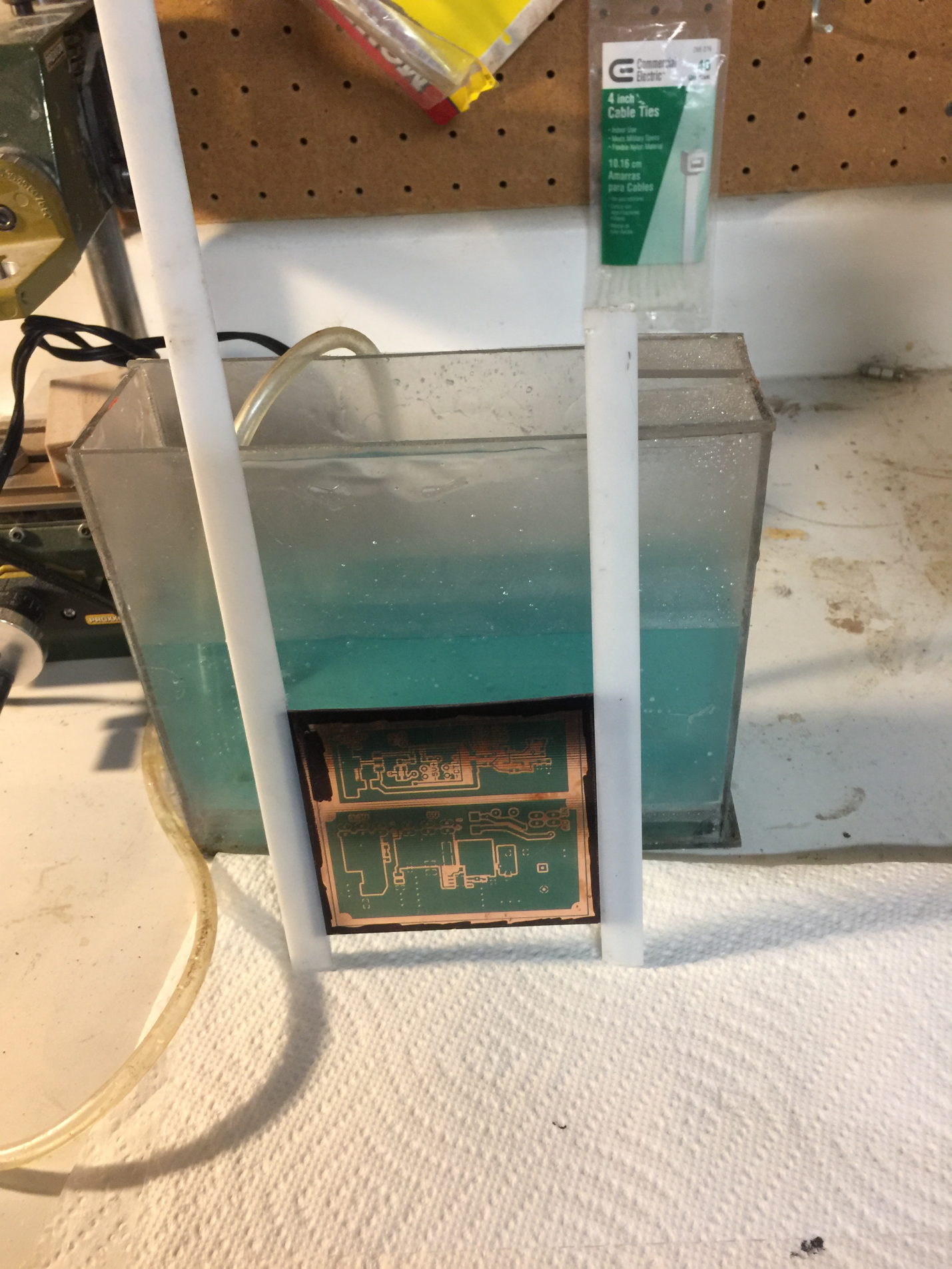
Next step is to take the artwork “sandwich” and I place it between 2 pieces of glass. I use 5” x 8” picture frame glass that I stole from a frame I got at Walmart. It also makes it easier if you rubber band the two glass halves together once the artwork is inside them. That way you only need to handle one “assembly” during development.
Here’s the artwork sandwich. Note: the white protective film is still in place on the PCB.
Okay, it’s finally time to expose the PCB to the UV light. First, I’ve found it’s important to warm up the light box. I believe that it takes a couple of minutes for the UV bulbs to warm up and stabilize their output. To do that, I simply turn on the light box for a couple minutes. You will not get consistent results if you skip this.
Next, you’re ready to remove the protective film from the PCB. I generally try to do this in low light, but I don’t think it’s terribly critical to be lightening fast. I generally peel back one corner about ¼” and then peel back a corner on the opposite side. When ready, I pull the film off of both sides, holding the board by the edges (don’t get fingerprints on the pre-sensitized board). I quickly insert the board into the artwork sandwich and then sandwich that in between the two glass sheets and rubber band them together. Next, I briefly shut off the light box which has been warming up. I place the glass assembly on the acrylic platform in the lightbox and cover the back with a piece of black plastic. I do this as a precaution to keep everything as flat as possible.
Next, I close the lid turn on the lightbox and start timing. In my case, once 2:30 is done, I flip the PCB sandwich over and expose the other side for the same amount of time. Once the timer is done, I turn off the lightbox and generally leave the PCB inside where it’s dark until I’m ready to wash it with developer.
Next step is to develop the board. This is another critical step. I’ve tried several developers. Most are based on sodium hydroxide, which is drain cleaner. I’ve never once had success – especially with a fine pitched surface mount component. They all overdevelop the board which means that too much of the mask is removed. It’s just too hard to control.
The only product I will use is this DP-50 availiable here: https://www.circuitspecialists.com/posdev.html
It’s cheap and easy to use. It is not prone to over developing and isn’t as harsh as sodium hydroxide.
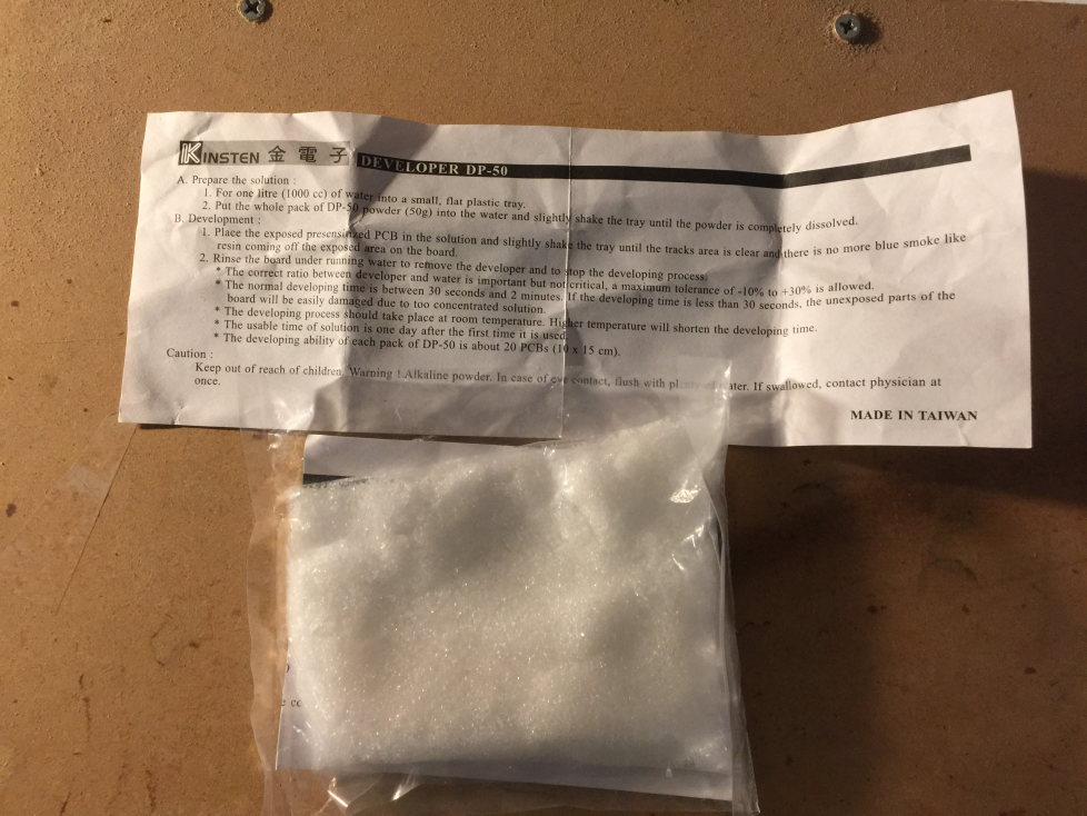
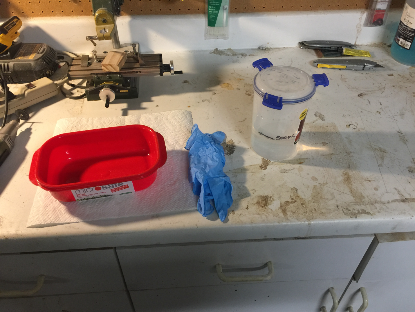
One package of the powder makes 1 Liter which is more than what is needed to develop a single board or two so I split packages into two 25 gram packs and mix up 500 mL at a time.
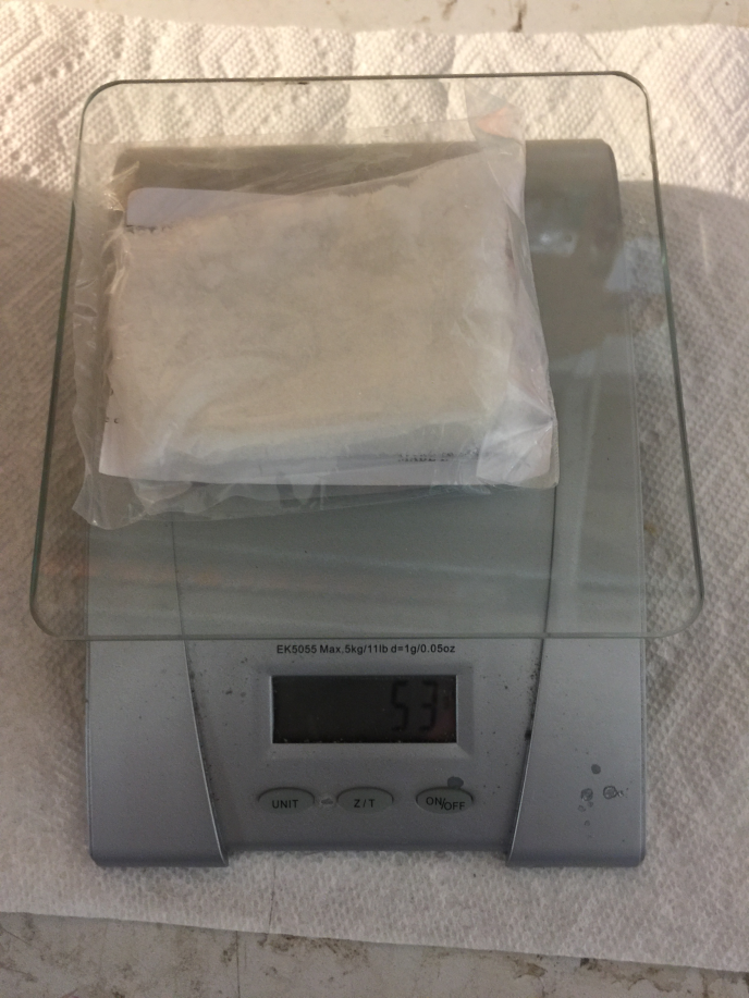
With the scale and development stuff my wife call it the meth lab.
Here’s the developing setup. I use a small plastic tray (from Walmart) and a mixing container that I have a 500mL mark drawn onto. It’s also a good idea to use gloves, although I’ll admit I haven’t always.
I premix the developer with warm water. I played around with this some, trying to improve the development process. The process only takes a minute, so reducing time is not the aim. I was simply trying to get finer and crisper lines on my PCB. If the developer solution is too cold, it takes longer and the results are not as uniform on the board. Bad! If the solution is warm, as I said, it only takes a minute. If the solution is super hot (ie boiling water) then the process is too fast…maybe a few seconds and impossible to control. Therefore, I simply use warm tap water…about the same temperature you’d wash your hands with.
Note: the developer does not store well. You can’t mix up a batch, make a board, then store and reuse it a few days/weeks/months later. I have successfully used it a few times the same day but beyond that I’ve had problems. Don’t be a cheap bastard (like me) and just mix up some new stuff.
To develop the board, I pour a few hundred mL into the tray and simply agitate the board by hand.
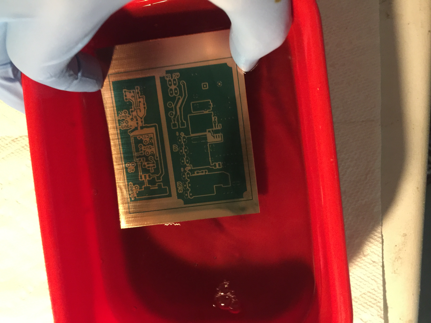
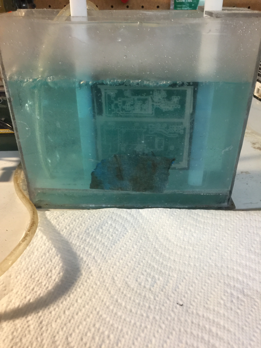
You’ll quickly see the unmasked copper come clear. Note: in the picture you can actually see the green mask washing off. Every 10 seconds or so I pull the board out. I look at the fin pitched surface mount pads to see if the developer has washed away between all the pins. If not, I flip the board and submerge and agitate for another 10 seconds or so and repeat. After a minute, you should stop seeing much change and the artwork should all look good. When you’re satisfied, wash the board in cool running water. I usually overdo it to ensure all the developer is washed off.
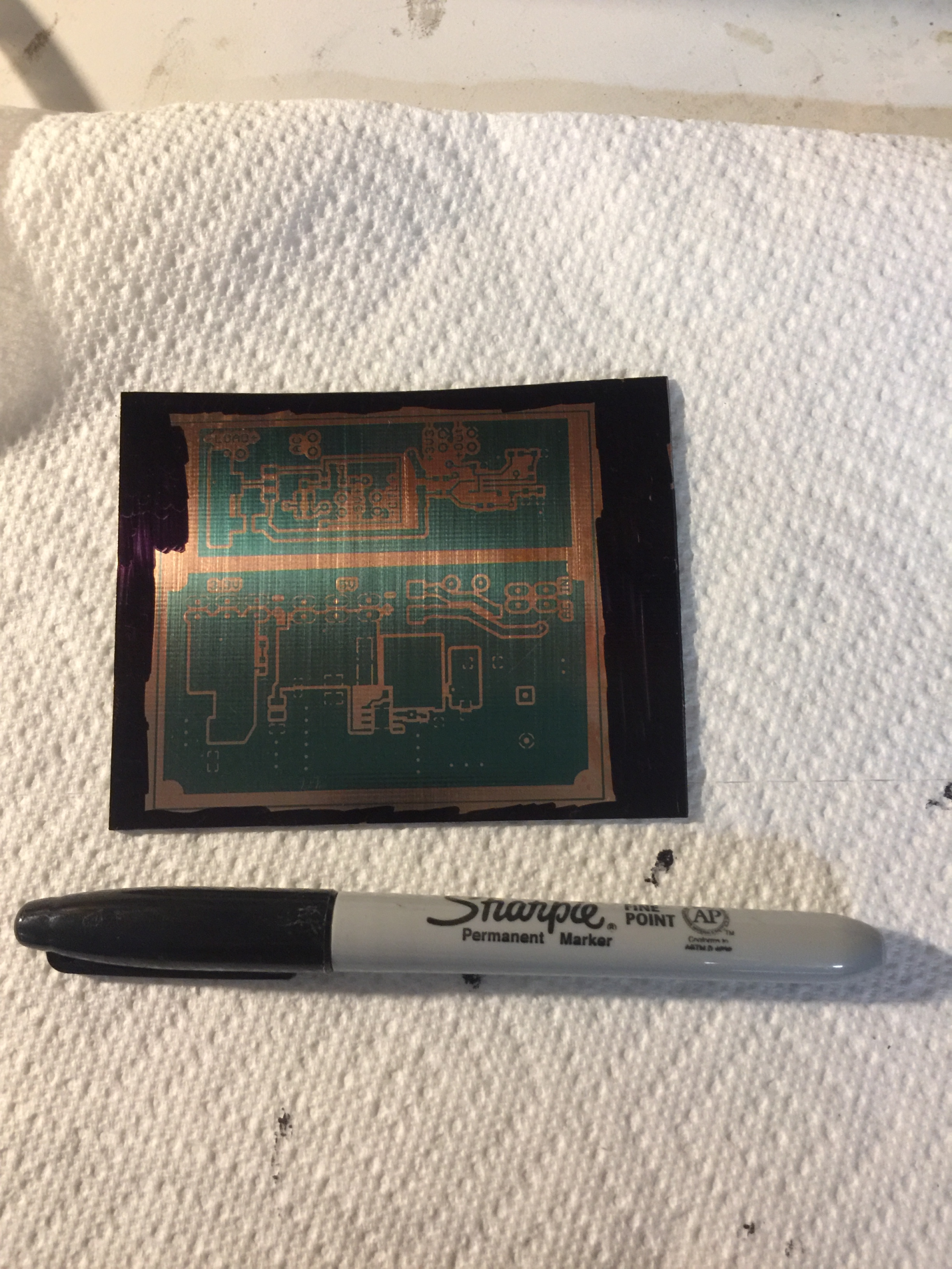
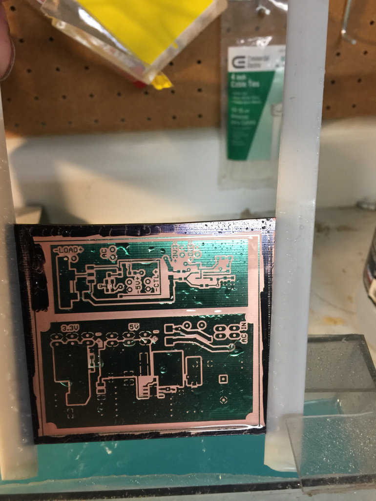
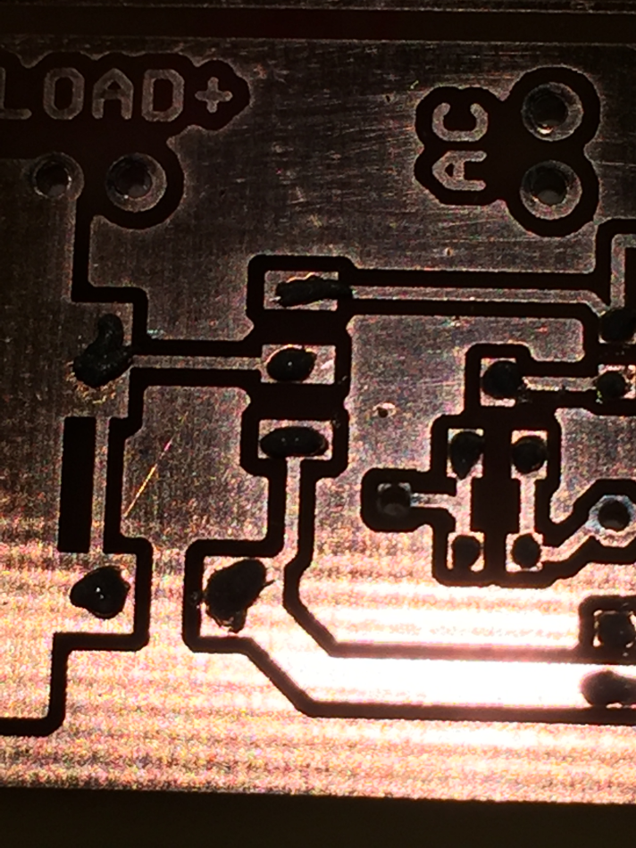
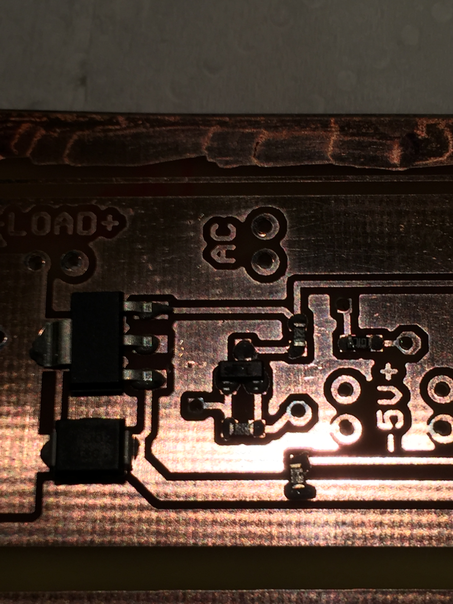
Next step is to get ready to develop the board. I usually carefully inspect the board under a microscope to look for artwork imperfections. Small ones can be fixed with a fine tip Sharpie. Sharpie ink does a great job as a resist and can fix broken traces and other problems. I also use it to color in around the board edges. I simply don’t want to use up etching solution stripping copper off of areas that I don’t care about.
.
Now it’s time to develop the board! I wish I had taken pictures of how I constructed my developer tank. Net, there are lots of nice tanks you can buy, however most are too big for the occasional PCB. I wanted a small tank that would be good for boards up to about 4”x4”. I also wanted agitation (bubbles) to help the etching process. I ended up making one out of the same acrylic sheeting I used on the lightbox. You can buy acrylic cement at a hobby store (i.e. Hobby Lobby). It reminds me of the sprinkler PVC cement in that it’s very forgiving and easy to use.
I’ll try to hand wave the construction and let you look at some pictures. The biggest problem was cutting the sheeting without splintering it. I tried blades, jig saws, circular saws, hack saws, etc. I tried so many different methods, I can’t remember which one worked best.
Here is a rough step by step construction guide
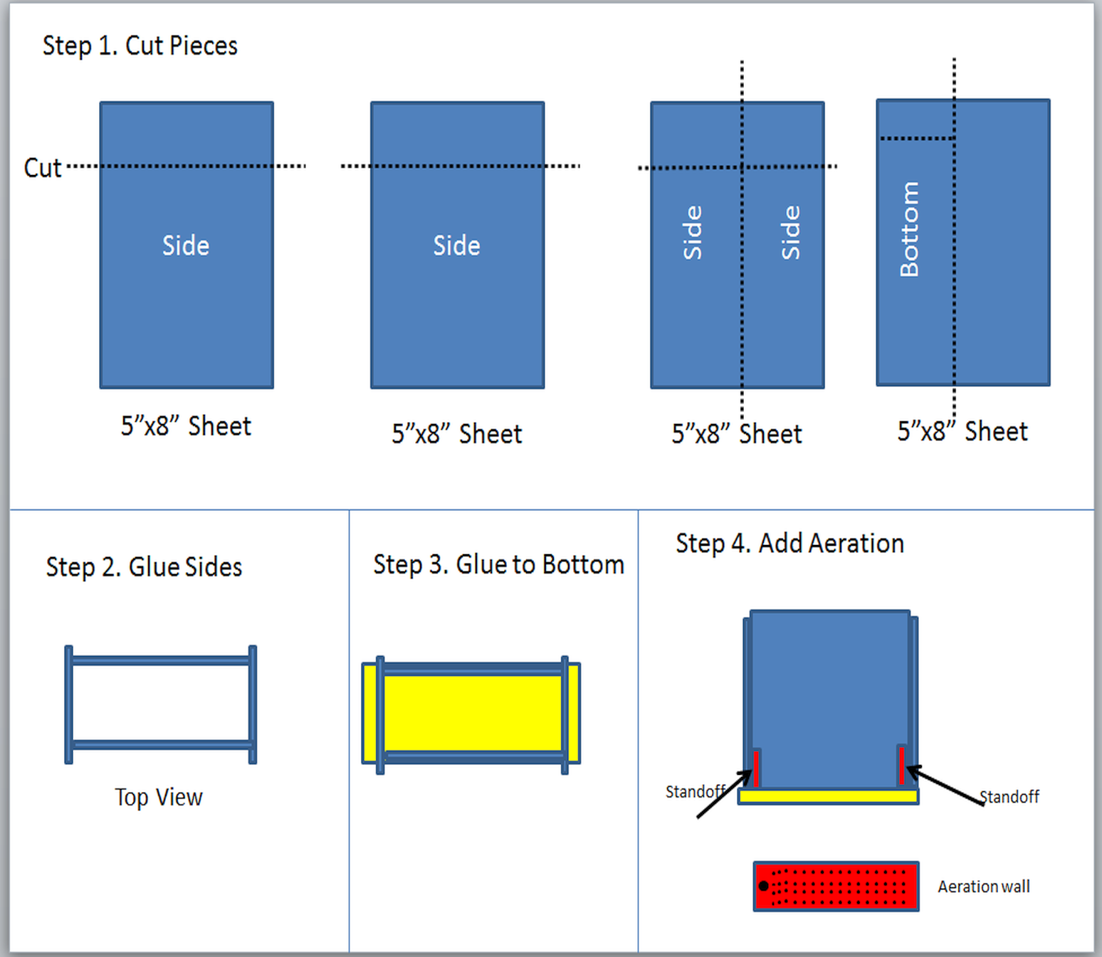
Start with 3 pieces of 5”x8” acrylic. Figure out the dimensions you want to use. The trick is to use as many flat and machined edges as possible. As an example, cut 2 sides each 5” x 6” as shown in step #1 above. This will require one cut edge and leave 3 machined edges. Next cut 2 sides, each 2.5” x 6”. Glue the 4 sides together with the short edges overlapping as in step 2. This will glue the machined edges of the 5” x 6” sides to the flat sides of the 2.5” x 6” sides, leaving an interior volume of roughly 2” x 5” x 6”. One way to do this is simply rubber band the 4 sides together, then run acrylic glue along their joints. Make sure the bottoms are all flush when gluing. Take the 4 sided assembly and set on the bottom. Again, the machined edges sit on the flat side of the bottom. Simply apply glue to joints. Once dry, add some water to look for leaks. On my first attempt I had some. I simply poured more glue over those areas until they were sealed up. Finally, I added the aeration chamber. I cut a couple standoffs from scrap acrylic, roughly 2” x 1” and glued them to the interior sides as shown in step 4. It’s not as easy as it sounds because your hand will probably not fit into the container. Then cut an aeration plenum which is roughly the same size as the interior i.e. 2” x 5”. Drill a ¼” hole. This will be for air tubing. Next drill a bunch of small holes ~ 1/8” for the air bubbles to escape. Finally glue in the plenum on top of the standoffs and seal edges with acrylic glue. It’s not critical to get a watertight seal there at all.
Get a fish aerator and ¼” tubing and feed the tubing through the ¼” hole in the plenum. Done.
Next problem is how to submerge the board in the etching solution. I ended up using plastic report cover clips like these: https://www.officedepot.com/a/products/678708/Office-Depot-Brand-Sliding-Bar-Report/
Here you can see a PCB board ready for etching with a clip attached to each edge. The clips allow the board to be submerged, agitated, rotated, etc.
In terms of etching solution, I like to use sodium Persulphate. It’s not cheap, but it’s not more expensive than Ferric Chloride. In this case it’s the lesser of two evils. Ferric Chloride is nasty, very corrosive, and stains everything. Sodium Persulphate is much easier to use and it turns a cool blue color as the etching process happens.
To use it, I simply follow the directions on mixing. I like to heat it up in a microwave prior to etching to get it good and hot (not boiling). Heating it up accelerates the etching process. Once I’m ready, I turn on the aeration, submerge the board, and twiddle my thumbs.
Every so often, pull the board out and take a look. At first the copper will become very dull.
As the process continues, the board areas will gradually become exposed. I keep a magnifying glass handy and inspect the small surface mount pins. Once everything I want is etched away, I take the board and wash it with cool tap water to stop the etching process.
That’s pretty much it from soup to nuts on how to etch your own boards. I’ve had several instances where I fail at one point in the process or another. I keep a checklist on my phone that I go through each time to ensure consistency. Whenever I’ve failed to make a board properly, I can always trace it back to missing a step in the process. Just learn from your mistakes like I have.
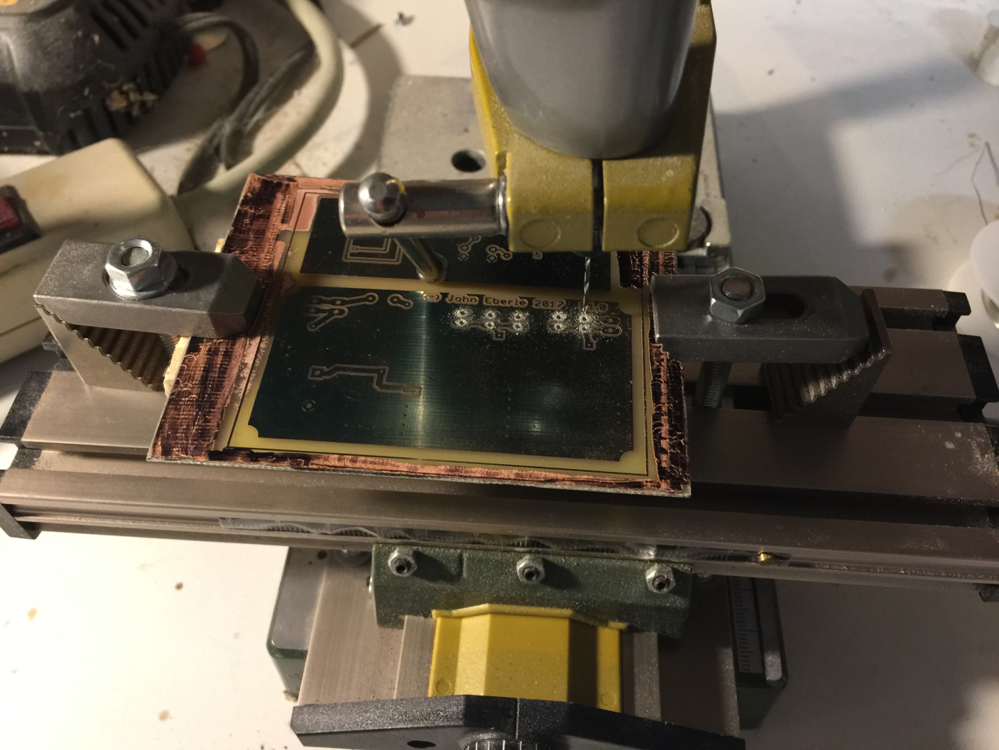
Next step in the fabrication process is drilling. It’s pretty straightforward. As I indicated earlier, I use a small drill press and X-Y table. The X-Y table allows me to set up the job and turn some dials to move from one hole to the next. It’s slow but not too difficult.
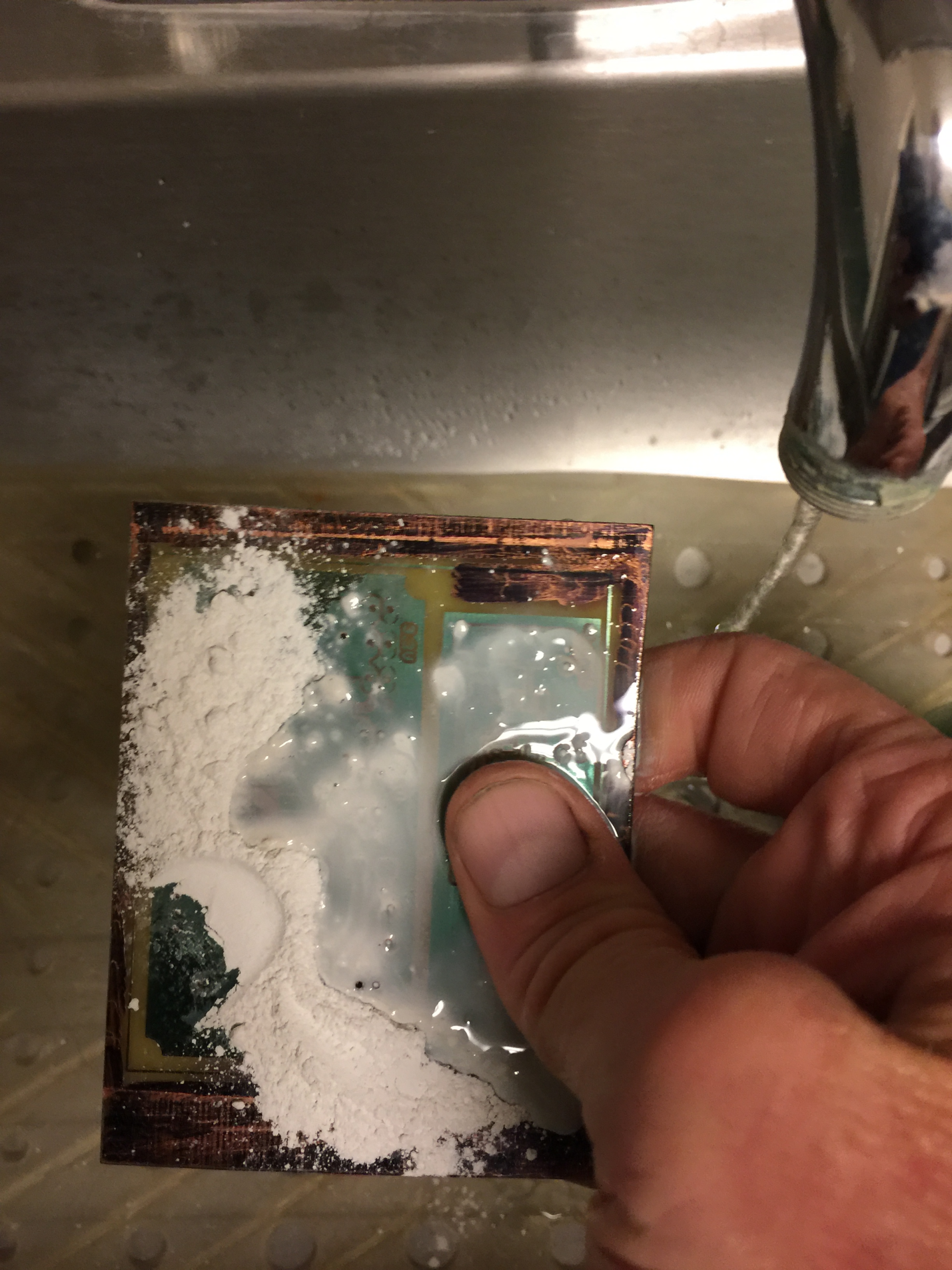
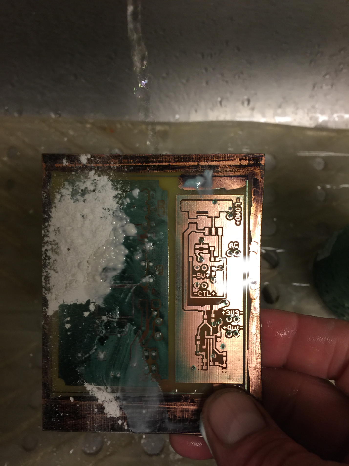
Now we’re getting close to soldering things up, but before that can happen the solder mask must be removed. I’ve tried a few ways, but I like using Comet cleanser the best. I put a little on the board, add water to make a paste, and start scrubbing. The abrasives in the cleanser clean off the board nicely. The only issues are: 1) it’s a fair amount of scrubbing and 2) you really have to wash the board well to get the cleanser out of the drill holes.
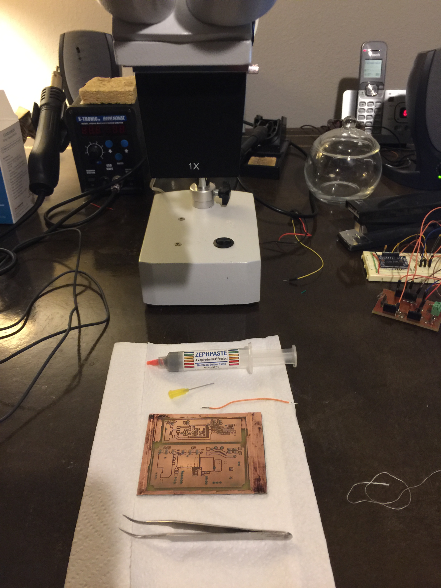
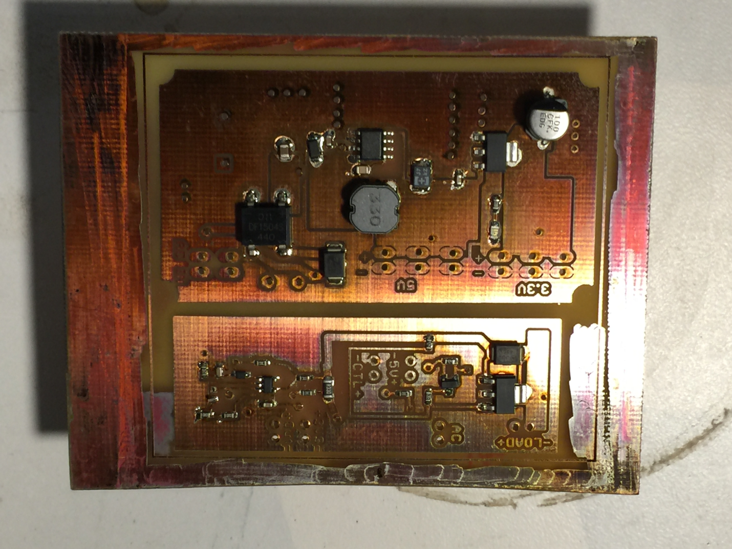
Once the board is nice and clean, it’s time to solder on the surface mount components. The copper will start to oxidize pretty much as soon as it’s cleaned off. Solder has flux in it to help break through the oxidation, however I try to get the soldering done as quickly as possible after cleaning. One of the really nice things about commercial boards is that they coat the boards with a resist which helps insulate the board and keep it from oxidizing. They also tin the contact points (I don’t actually know if it’s a tinning process) to allow corrosion free joints.
Time to start placing the solder paste and components. As I indicated earlier, I don’t use stencils, which requires me to manually put solder on each pad. It’s very labor intensive and it can be messy. I’m pretty sure a stencil provides superior coverage and results. I will likely try them on my next decent size board.
Here you can see a view with the small dots of solder paste I put down with a fine dispenser tip. Here’s the good news, the solder will “flow” when it heats up. The flowing action will draw the solder (and the parts) to the pads. If you accidentally “make a mess” and get solder paste across two adjacent pads, the problem will likely fix itself during the reflow process. I’ve place 44 pin microprocessors with .6mm spaced leads where virtually every pin is bridged with solder paste, but once the reflow process happens the solder sucks in and all the joints are perfect.
Here’s the board with the components on the solder paste.
I’ve done a few large boards where I can’t place all the components in one sitting. Generally I get started on them at 9:30 pm work till midnight, then go to bed and work the next day and so it gets to be the next night before I continue. In these cases I simply put the board in the refrigerator. It keeps the solder paste from drying out too fast.
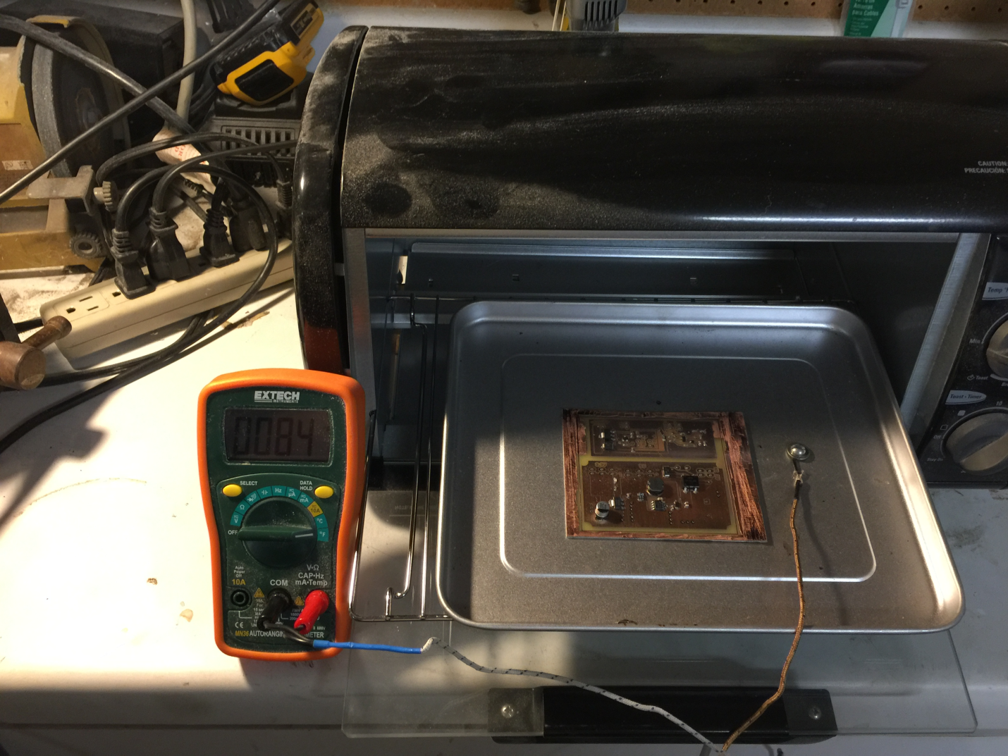
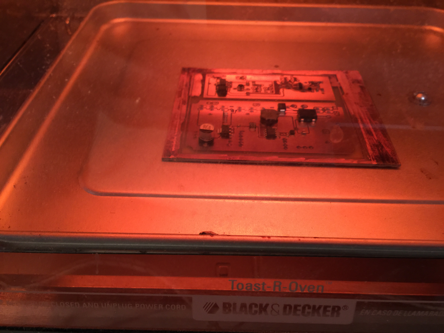
To actually do the reflow, I use a toaster oven. I have a DVM which has a thermocouple on it which I mount in the oven. I roughly follow a reflow progression as best as possible. First I warm to about 120F and let everything equilibrate for a couple minutes.
I modulate the temperature in the toaster oven by turning it on/off and by opening and closing the door manually. It’s another story, but I built an oven controller and it turns out to be very difficult to control the heating. The heat load is very small and the toaster can supply a lot of heat. The process integrates very quickly and the overshoot is rather dramatic. Opening the door is the best way to remove the excess heat and provides a control mechanism. If I were to build another controller, I’d add some dampers and/or fans to provide control. …Too many projects and not enough time.
After equilibration I generally bring it up to about 220F and pause for a minute. Then I allow the oven to heat up to 450F. I generally turn off the heating elements at 400F and allow the thermal inertia (is that the right term???) to carry the temperature up to 450F. At 450F I open the door which starts the cooling process, being careful not to jar the board since the components are not set. I watch the temperature, sometimes gently blowing into the oven to accelerate the cooling, until it drops back to < 150F at which point the board is safe to grab.
Next job is to mount the through hole components and feed wire through the vias. How to do the through hole components is obvious. I’ve found the best way to do the vias is to buy bare hook up wire (26 gauge I think). Cut a piece a few feet long and start threading through the vias like you’re sewing them together. When you have 5-10 of them hooked together, start soldering tops and bottoms. When you’re done (or as you go along) the wire can be trimmed at the top and bottom of each via to complete it.
That’s all there is to it. Enjoy!